| CPC H01G 4/248 (2013.01) [H01G 4/30 (2013.01); H05K 1/181 (2013.01)] | 11 Claims |
|
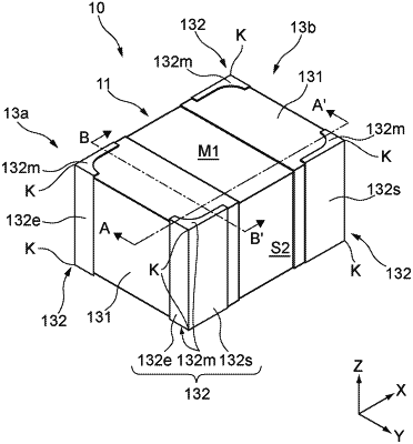
1. A multi-layer ceramic electronic component, comprising:
a ceramic body including
a main surface, an end surface, and a side surface that are respectively perpendicular to a first axis, a second axis, and a third axis orthogonal to one another,
a top portion that connects the main surface, the end surface, and the side surface to one another, and
a plurality of internal electrodes laminated in a direction of the first axis; and
an end external electrode including
a corner portion located on the top portion,
a base portion that covers the end surface and extends from the end surface to the main surface and the side surface, and
a protrusion that protrudes from the base portion in a thickness direction, the protrusion including an L-shaped main surface protrusion that is located on the main surface and extends in a direction of the second axis and in a direction of the third axis from the corner portion.
|