US 11,929,141 B2
Sparsity-aware reconfigurable compute-in-memory (CIM) static random access memory (SRAM)
Kaushik Roy, West Lafayette, IN (US); Amogh Agrawal, West Lafayette, IN (US); Mustafa Fayez Ahmed Ali, West Lafayette, IN (US); Indranil Chakraborty, West Lafayette, IN (US); Aayush Ankit, West Lafayette, IN (US); and Utkarsh Saxena, West Lafayette, IN (US)
Assigned to Purdue Research Foundation, West Lafayette, IN (US)
Filed by Purdue Research Foundation, West Lafayette, IN (US)
Filed on Dec. 8, 2021, as Appl. No. 17/643,215.
Prior Publication US 2023/0178125 A1, Jun. 8, 2023
Int. Cl. H03M 1/12 (2006.01); G11C 7/10 (2006.01); G11C 7/16 (2006.01)
CPC G11C 7/16 (2013.01) [G11C 7/1012 (2013.01); G11C 7/1063 (2013.01); G11C 7/109 (2013.01); H03M 1/1245 (2013.01)] 17 Claims
OG exemplary drawing
 
1. A memory circuit comprising:
a memory array comprising a plurality of memory cells;
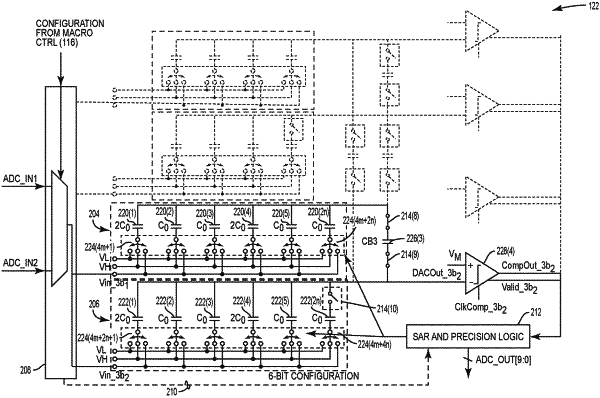
an analog-to-digital converter (ADC) comprising:
a first m-bit sub-ADC; and
a first n-bit sub-ADC, wherein n does not equal m; and
a control circuit coupled to the memory array, the control circuit configured to:
determine a workload sparsity level;
based on the workload sparsity level, determine a bit-precision requirement; and
based on the bit-precision requirement, activate the first m-bit sub-ADC, the first n-bit sub-ADC, or both.