| CPC G11C 29/54 (2013.01) [G11C 29/56004 (2013.01)] | 10 Claims |

|
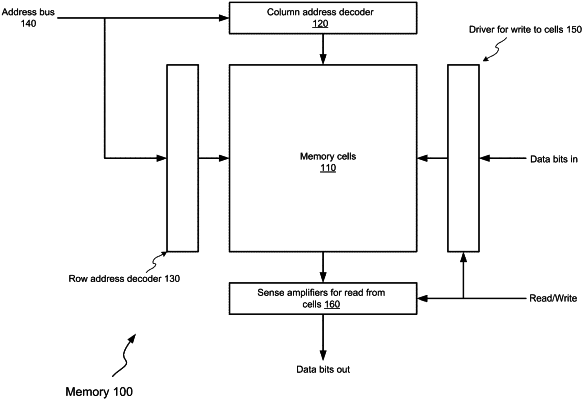
1. A memory-testing circuit in a circuit configured to perform a test of a memory in the circuit, the memory comprising: data bit columns configured to store data bits, reference bit columns configured to store reference bits, and column association circuitry configured to associate one or more of the reference bit columns with a data bit column in the data bit columns, the memory-testing circuit comprising:
a test controller;
association adjustment circuitry coupled to the column association circuitry and the test controller, the association adjustment circuitry configurable by the test controller to associate another one or more of the reference bit columns or one or more of the data bit columns with the data bit column in the data bit columns; and
repair circuitry configured to use extra reference bit columns to replace defective reference bit columns detected by the memory-testing circuit, the repair circuitry comprises:
a register coupled to the association adjustment circuitry and configured to load repair information for one or more defective reference columns,
an address comparison device configured to compare a data bit column address for a read operation with an address or addresses for data bit columns associated with the one or more defective reference bit columns, and
a multiplexing device controlled by an output of the address comparison device and configured to select an output signal from between a signal from the register and a signal from the column association circuitry,
wherein the test of the memory comprises:
performing one or more read operations based on one or more of the reference bit columns associated by the column association circuitry to generate one or more outputs,
comparing the one or more outputs with corresponding good-machine values to determine whether any of the one or more outputs is incorrect,
if at least one of the one or more outputs is incorrect, repeating at least one of the one or more read operations that generates the at least one of the one or more outputs based on another one or more of the reference bit columns or one or more of the data bit columns which are associated by the association adjustment circuitry to generate at least one second output, and
comparing the at least one second output with the corresponding good machine value to determine whether the one or more of the reference bit columns associated by the column association circuitry have a defect.
|