| CPC G11C 16/3459 (2013.01) [G11C 16/0483 (2013.01); G11C 16/10 (2013.01); G11C 16/24 (2013.01)] | 19 Claims |
|
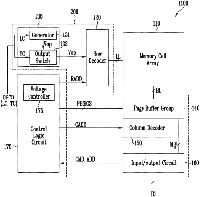
1. A memory device, comprising:
a memory block in which a plurality of cell pages are coupled to each of word lines;
a peripheral circuit configured to adjust a time point at which a verify voltage is applied to a selected word line among the word lines according to an order of performing a program operation during a verify operation of a selected cell page; and
a control logic circuit configured to transmit, to the peripheral circuit, an operation code for adjusting the time point at which the verify voltage is output.
|