| CPC G11C 16/14 (2013.01) [G11C 16/24 (2013.01); G11C 16/26 (2013.01); G11C 16/30 (2013.01); G11C 16/32 (2013.01); G11C 16/3445 (2013.01)] | 18 Claims |
|
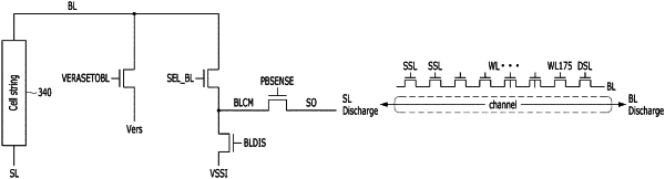
1. A memory device, comprising:
a cell string including plural non-volatile memory cells which are capable of storing data, the cell string arranged between a bit line and a source line;
plural first discharge transistors coupled in parallel to the source line for providing a first current path of discharging the charges;
at least one second discharge transistor coupled to the bit line for providing a second current path of discharging charges which are accumulated in a channel formed through the cell string; and
a control circuit configured to control the plural first discharge transistors and the at least one second discharge transistor for synchronizing discharge of the charges via the first and second current paths, the bit line, and the source line during an erase operation for erasing the data stored in the plural non-volatile memory cells.
|