| CPC G09G 3/32 (2013.01) [H01L 25/167 (2013.01); H01L 27/124 (2013.01); H03K 5/01 (2013.01); G09G 2300/0426 (2013.01); G09G 2300/0861 (2013.01); G09G 2310/0291 (2013.01); G09G 2310/06 (2013.01); G09G 2310/08 (2013.01); G09G 2330/028 (2013.01)] | 20 Claims |
|
1. An apparatus for manufacturing a display device, comprising:
a stage;
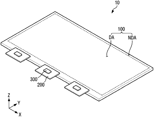
a panel cell disposed on the stage and including:
a first alignment line; and
a second alignment line extending parallel to the first alignment line;
a field application part providing an alignment signal to the first alignment line and the second alignment line of the panel cell; and
light-emitting elements aligned between the first alignment line and the second alignment line,
wherein the field application part provides an alignment signal to the first alignment line and the second alignment line, the alignment signal having the same positive integral value and negative integral value, having a different positive peak voltage from the alignment signal's negative peak voltage, and having a different positive pulse width from the alignment signal's negative pulse width.
|