| CPC G06F 7/50 (2013.01) [H01L 23/535 (2013.01); H10B 41/27 (2023.02); H10B 41/41 (2023.02); H10B 43/27 (2023.02); H10B 43/40 (2023.02)] | 20 Claims |
|
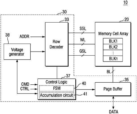
1. A semiconductor memory device comprising:
a memory cell region including a memory cell array; and
a peripheral circuit region which at least partially overlaps the memory cell region and includes control logic configured to control operation of the memory cell array,
wherein the control logic includes
a state machine configured to output a plurality of state signals responsive to operation commands of the memory cell region, the plurality of state signals including a first state signal output from a first output terminal, and a second state signal output from a second output terminal different from the first output terminal,
a logical sum calculator configured to perform a logical sum calculation based on at least one of the first state signal or the second state signal, and
an accumulation circuit configured to receive an output of the logical sum calculator as a clock signal, and that outputs a toggle signal to one probing pad in response to the clock signal, the accumulation circuit being connected to the probing pad through a Through Hole Via (THV) penetrating the memory cell region.
|