| CPC G06F 3/0659 (2013.01) [G06F 3/0604 (2013.01); G06F 3/0679 (2013.01)] | 4 Claims |
|
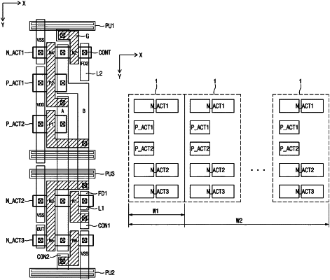
1. A fuse latch of a semiconductor device comprising:
a data transmission circuit configured to transmit data to a first node and a second node in response to a first control signal and to include a first NMOS transistor and a second NMOS transistor;
a latch circuit configured to latch the data received from the data transmission circuit through the first node and the second node and to include a first PMOS transistor, a third NMOS transistor, a second PMOS transistor, and a fourth NMOS transistor; and
a data output circuit configured to output the data latched by the latch circuit in response to a second control signal and to include a fifth NMOS transistor and a sixth NMOS transistor,
wherein at least a portion of the first to sixth NMOS transistors are disposed in first, fourth, and fifth active regions, the first and second PMOS transistors are disposed in second and third active regions, and the first to fifth active regions are sequentially arranged in a first direction,
wherein the first to sixth NMMOS transistors are arranged in two columns in each of the first, fourth, and fifth active regions along a second direction intersecting the first direction; and
wherein the first and second PMOS transistors are arranged in one column in each of the second and third active regions along the second direction.
|