| CPC G06F 3/0632 (2013.01) [G06F 3/0604 (2013.01); G06F 3/064 (2013.01); G06F 3/0679 (2013.01); G11C 16/26 (2013.01)] | 20 Claims |
|
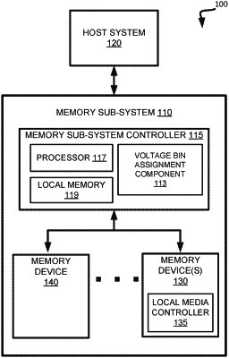
1. A system comprising:
a memory device; and
a processing device, operatively coupled to the memory device, to perform operations comprising:
sorting a plurality of blocks of the memory device;
identifying, based on scanning of a first block at a first location of the plurality of sorted block, a first voltage bin associated with the first block;
identifying, based on scanning of a second block at a second location of the plurality of sorted blocks, a second voltage bin associated with the second block; and
responsive to determining that the first voltage bin matches the second voltage bin, assigning the first voltage bin to each block that is located between the first location of the plurality of sorted blocks and the second location of the plurality of sorted blocks.
|