| CPC G06F 3/0445 (2019.05) [G06F 3/0446 (2019.05)] | 18 Claims |
|
1. A display device, comprising:
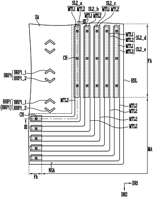
a substrate including a display area and a non-display area;
pixels provided in the display area of the substrate;
an encapsulation layer disposed on the pixels;
a first conductive pattern disposed on the encapsulation layer, the first conductive pattern including a first metal layer of sensing lines disposed in a non-sensing area corresponding to the non-display area;
a first insulating layer disposed on the first conductive pattern;
a second conductive pattern disposed on the first insulating layer, the second conductive pattern including a second metal layer of the sensing lines disposed in the non-sensing area; and
a second insulating layer disposed on the second conductive pattern,
wherein the first metal layer includes a first end located in the non-sensing area corresponding to a first side of a sensing area, the sensing area corresponding to the display area, and a second end located in the non-sensing area corresponding to a second side adjacent to the first side, and
wherein the first metal layer is disconnected between the first end and the second end, such that a portion of the encapsulation layer is exposed from the first metal layer between the first end and the second end.
|