| CPC G06F 3/0445 (2019.05) [G06F 3/0412 (2013.01); G06F 3/0446 (2019.05); H10K 59/40 (2023.02); G06F 2203/04102 (2013.01); G06F 2203/04105 (2013.01); G06F 2203/04112 (2013.01); H10K 59/122 (2023.02)] | 18 Claims |
|
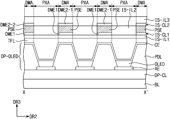
1. A display device comprising:
a display panel configured to display an image on a display surface; and
an input sensor having a sensor area and a dummy area,
wherein the input sensor includes:
a first conductive layer disposed on the display panel, the first conductive layer including a first dummy electrode disposed in the sensor area and the dummy area;
a second conductive layer disposed on the first conductive layer, the second conductive layer including a sensor electrode disposed in the sensor area and a second dummy electrode disposed in the dummy area; and
a pressure sensor electrode disposed between the first conductive layer and the second conductive layer, and disposed between the first dummy electrode and the second dummy electrode to overlap the first dummy electrode and the second dummy electrode in a plan view.
|