| CPC G06F 3/0443 (2019.05) [G06F 3/0412 (2013.01); G06F 3/04164 (2019.05)] | 21 Claims |
|
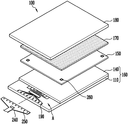
1. A display device comprising:
a display panel including a display area and a non-display area;
a sensing unit disposed on the display area of the display panel, wherein the sensing unit includes sensor electrodes, a connecting part electrically connecting adjacent sensor electrodes, a first insulating layer disposed between the sensor electrodes and the connecting part, and a second insulating layer disposed on the sensor electrodes and the connecting part; and
a mark overlapping the non-display area and including a first pattern part formed in a same conductive layer as the sensor electrodes and a second pattern part formed in a same conductive layer as the connecting part, and
wherein at least one of the first insulating layer and the second insulation layer includes an opening exposing at least a portion of the first pattern part, and
wherein the second pattern part overlaps the second insulating layer in a thickness direction.
|