| CPC G06F 16/116 (2019.01) [G06F 16/285 (2019.01)] | 20 Claims |
|
1. A data storage device comprising:
a controller comprising:
a processor configured to control a read or write operation based on a command received from an external device; and
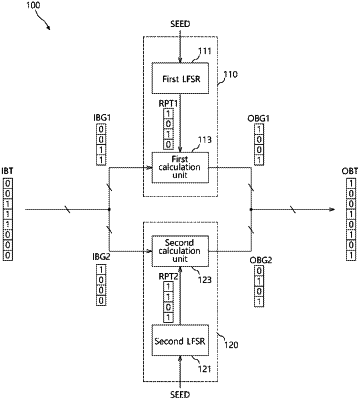
a data processing circuit configured to randomize a plurality of input bit groups to output output bits including a transformed input bit group based on a seed received from the processor and a polynomial; and
a nonvolatile memory configured to write the output bits at a memory region according to an address offset,
wherein the seed has a relationship to the address offset and the polynomial has a degree which is an integral multiple of a total number of input bits in the input bit groups provided tothe data processing circuit and the seed corresponding to each memory region having relationship to the address offset is fixed.
|