US 11,928,020 B2
Memory error detection
Ian Shaeffer, Los Gatos, CA (US); and Craig E. Hampel, Los Altos, CA (US)
Assigned to Rambus Inc., San Jose, CA (US)
Filed by Rambus Inc., San Jose, CA (US)
Filed on Jan. 10, 2023, as Appl. No. 18/095,341.
Application 18/095,341 is a continuation of application No. 17/481,246, filed on Sep. 21, 2021, granted, now 11,579,965.
Application 17/481,246 is a continuation of application No. 16/678,159, filed on Nov. 8, 2019, granted, now 11,150,982, issued on Oct. 19, 2021.
Application 16/678,159 is a continuation of application No. 15/838,161, filed on Dec. 11, 2017, granted, now 10,558,520, issued on Feb. 11, 2020.
Application 15/838,161 is a continuation of application No. 14/864,500, filed on Sep. 24, 2015, granted, now 9,870,283, issued on Jan. 16, 2018.
Application 14/864,500 is a continuation of application No. 14/200,665, filed on Mar. 7, 2014, granted, now 9,170,894, issued on Oct. 27, 2015.
Application 14/200,665 is a continuation of application No. 14/020,755, filed on Sep. 6, 2013, granted, now 8,707,110, issued on Apr. 22, 2014.
Application 14/020,755 is a continuation of application No. 13/666,918, filed on Nov. 1, 2012, granted, now 8,555,116, issued on Oct. 8, 2013.
Application 13/666,918 is a continuation of application No. 12/424,094, filed on Apr. 15, 2009, granted, now 8,352,805, issued on Jan. 8, 2013.
Application 12/424,094 is a continuation in part of application No. 12/035,022, filed on Feb. 21, 2008, granted, now 7,836,378, issued on Nov. 16, 2010.
Application 12/035,022 is a continuation of application No. 11/436,284, filed on May 18, 2006, abandoned.
Prior Publication US 2023/0333927 A1, Oct. 19, 2023
This patent is subject to a terminal disclaimer.
Int. Cl. G06F 11/00 (2006.01); G06F 11/07 (2006.01); G06F 11/10 (2006.01); G06F 11/16 (2006.01); H03M 13/09 (2006.01)
CPC G06F 11/1004 (2013.01) [G06F 11/0703 (2013.01); G06F 11/073 (2013.01); G06F 11/1679 (2013.01); H03M 13/09 (2013.01)] 20 Claims
OG exemplary drawing
 
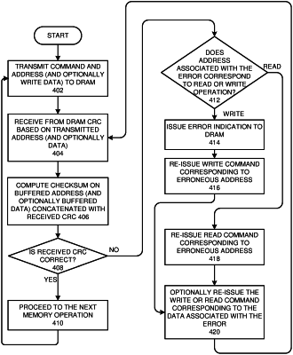
1. A memory controller to control memory, the memory controller comprising:
circuitry to transmit, to the memory, a write command and an associated address;
circuitry to generate error detection information, dependent on the associated address;
circuitry to detect, using the error detection information and additional information received from the memory, whether the associated address as received by the memory contains an error; and
circuitry to transmit to the memory, after a delay time with respect to the write command, a second communication, wherein the second communication upon receipt by the memory will cause the memory to store write data associated with the write command into a storage array of the memory.