| CPC G06F 1/3296 (2013.01) [G06F 1/06 (2013.01); G06F 1/3206 (2013.01)] | 15 Claims |
|
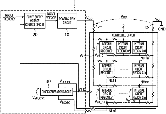
1. A voltage control device, comprising:
a power supply circuit configured to supply electric power to an input terminal of a controlled circuit;
a power supply voltage control circuit configured to control a power supply voltage to be supplied from the power supply circuit to the controlled circuit, based on a clock signal to be supplied to the controlled circuit; and
a clock generation circuit configured to:
receive a power supply that is an internal voltage to be applied to a second internal circuit region at a second wiring distance from the input terminal, and
generate the clock signal based on the internal voltage, wherein
the second wiring distance is longer than a first wiring distance at which a first internal circuit region is located in the controlled circuit, and
the first wiring distance and the second wiring distance corresponds to wiring distances in the controlled circuit from the input terminal.
|