US 11,927,982 B2
Keeper-free integrated clock gate circuit
Gururaj K. Shamanna, Austin, TX (US); Naveen Kumar M, Bengaluru (IN); Harishankar Sahu, Bangalore (IN); Abhishek Chouksey, Bengaluru (IN); and Madhusudan Rao, Bengaluru (IN)
Assigned to INTEL CORPORATION, Santa Clara, CA (US)
Filed by Intel Corporation, Santa Clara, CA (US)
Filed on Dec. 23, 2020, as Appl. No. 17/132,904.
Claims priority of application No. 202041031300 (IN), filed on Jul. 22, 2020.
Prior Publication US 2022/0026945 A1, Jan. 27, 2022
Int. Cl. G06F 1/10 (2006.01); G06F 1/08 (2006.01); H03K 19/20 (2006.01); H03K 3/037 (2006.01)
CPC G06F 1/10 (2013.01) [G06F 1/08 (2013.01); H03K 19/20 (2013.01); H03K 3/037 (2013.01)] 22 Claims
OG exemplary drawing
 
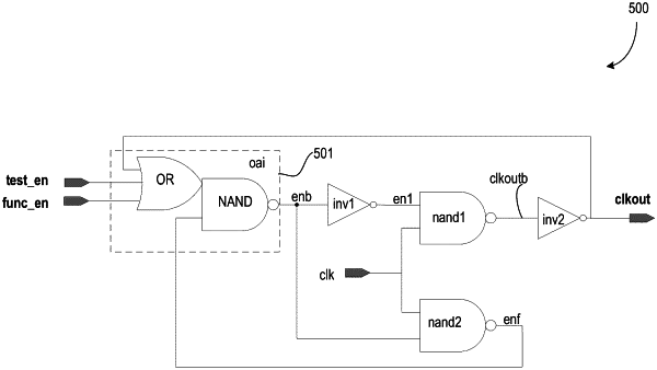
1. An apparatus comprising:
an OR-AND-INVERT gate to receive a first enable and a second enable;
a first inverter coupled to an output of the OR-AND-INVERT gate;
a first NAND gate coupled to the output of the first inverter;
a second NAND gate coupled to the output of the OR-AND-INVERT gate; and
a second inverter to provide a clock which is gated based on logic values of the first enable and/or the second enable, wherein an output of the second inverter is received as input by the OR-AND-INVERT-gate.