| CPC G02F 1/1368 (2013.01) [G02F 1/133345 (2013.01); G02F 1/136227 (2013.01); G02F 1/136286 (2013.01); G09G 3/3622 (2013.01); H01L 27/1225 (2013.01); H01L 27/1244 (2013.01); H01L 29/45 (2013.01); H01L 29/7869 (2013.01); G02F 1/13606 (2021.01); G02F 1/13624 (2013.01); G02F 1/136295 (2021.01); G02F 2202/10 (2013.01); G09G 2300/0426 (2013.01)] | 4 Claims |
|
1. A display device comprising:
a first pixel electrically connected to a signal line and a first scan line, wherein the first pixel comprises a first transistor and a pixel electrode electrically connected to the first transistor; and
a second pixel adjacent to the first pixel, the second pixel electrically connected to the signal line and a second scan line,
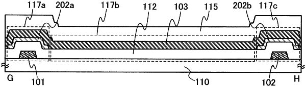
wherein no conductive layer is provided under the signal line in a region between the first scan line and the second scan line,
wherein the first transistor comprises:
a gate layer comprising copper;
a first insulating layer over the gate layer, the first insulating layer comprising silicon and nitrogen;
a second insulating layer over the first insulating layer, the second insulating layer comprising silicon and oxygen; and
an oxide semiconductor layer over and in contact with a top surface of the second insulating layer, the oxide semiconductor layer comprising indium, gallium, and zinc,
wherein a third insulating layer is positioned over and in contact with a top surface of the oxide semiconductor layer, the third insulating layer comprising silicon and oxygen,
wherein the oxide semiconductor layer comprises a channel formation region of the first transistor,
wherein the signal line comprises:
a first conductive layer comprising any one of titanium, molybdenum, and tungsten; and
a second conductive layer over the first conductive layer, the second conductive layer comprising copper,
wherein the signal line comprises a first region comprising a convex shape and a second region comprising a convex shape,
wherein the signal line and the first scan line intersect in the first region,
wherein the signal line and the second scan line intersect in the second region,
wherein the signal line is substantially entirely flat in the region between the first region and the second region,
wherein the signal line and the oxide semiconductor layer overlap each other in the first region,
wherein the first conductive layer comprises a region in contact with the top surface of the oxide semiconductor layer in the first region, and
wherein the signal line comprises a region not overlapping with the oxide semiconductor layer, in the region between the first region and the second region.
|