| CPC G02F 1/1368 (2013.01) [G02F 1/133345 (2013.01); G02F 1/13338 (2013.01); G02F 1/134336 (2013.01); G02F 1/13454 (2013.01); G02F 1/136286 (2013.01); G03F 7/70 (2013.01); G06F 3/0412 (2013.01); G02F 2201/42 (2013.01); G02F 2202/10 (2013.01); G06F 3/04164 (2019.05); G06F 3/044 (2013.01)] | 24 Claims |
|
1. An active matrix substrate comprising:
a substrate;
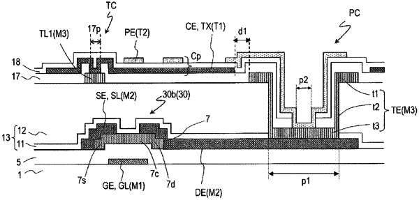
a plurality of thin film transistors supported on the substrate, each of the plurality of thin film transistors including a gate electrode formed of a first conductive film, a gate insulating layer covering the gate electrode, an oxide semiconductor layer arranged on the gate insulating layer, and a source electrode and a drain electrode formed of a second conductive film, the source electrode being in contact with a part of an upper face of the oxide semiconductor layer, the drain electrode being in contact with another part of the upper face of the oxide semiconductor layer;
an interlayer insulating layer covering the plurality of thin film transistors;
a plurality of pixel electrodes arranged above the interlayer insulating layer;
a common electrode including a plurality of common electrode portions arranged between the plurality of pixel electrodes and the interlayer insulating layer, each of the plurality of common electrode portions being configured to function as a first electrode for a touch sensor;
a first dielectric layer arranged between the interlayer insulating layer and the common electrode, and formed of a first dielectric film;
a second dielectric layer arranged between the common electrode and the plurality of pixel electrodes;
a plurality of touch wiring lines for touch sensors arranged between the interlayer insulating layer and the common electrode, and formed of a third conductive film; and
a plurality of pixel contact portions, each of the plurality of pixel contact portions electrically connecting one of the plurality of pixel electrodes to a corresponding one of the plurality of thin film transistors,
wherein each of the plurality of pixel contact portions includes
the drain electrode of the one of the plurality of thin film transistors,
the interlayer insulating layer including a lower opening exposing part of the drain electrode,
a connection electrode electrically connected to the drain electrode in the lower opening,
the first dielectric layer and the second dielectric layer including an upper opening exposing part of the connection electrode, and
the one of the plurality of pixel electrodes electrically connected to the connection electrode in the upper opening, and
the connection electrode is formed of the third conductive film.
|