| CPC G02F 1/1368 (2013.01) [H10K 59/124 (2023.02); H10K 71/00 (2023.02); H10K 59/1201 (2023.02)] | 13 Claims |
|
1. A display device comprising:
a transistor; and
a display element over the transistor;
wherein the transistor includes:
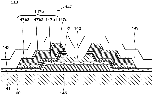
a gate electrode on an insulating surface;
a gate insulating layer on the gate electrode;
an oxide semiconductor layer arranged on the gate insulating layer, and overlapping the gate electrode;
source/drain electrodes, each of the source/drain electrodes including a first conductive layer above the oxide semiconductor layer, a second conductive layer on the first conductive layer, and a third conductive layer between the first conductive layer and the oxide semiconductor layer; and
an insulating layer overlapping the first to third conductive layers, the oxide semiconductor layer, and the gate electrode, the insulating layer containing oxygen and being on and in physical contact with a top surface of the first conductive layer,
wherein the first conductive layer contains titanium and nitrogen,
the second conductive layer contains a metal material,
the third conductive layer contains titanium, oxygen, and a part of the metal materials contained in the oxide semiconductor layer,
the first and second conductive layers are not in physical contact with the oxide semiconductor layer, and
the third conductive layer is on and in physical contact with the oxide semiconductor layer.
|