| CPC G02F 1/133526 (2013.01) [G02F 1/133512 (2013.01); G02F 1/133553 (2013.01); G02F 1/133638 (2021.01); G02F 1/13439 (2013.01); G02F 2413/01 (2013.01); G02F 2413/05 (2013.01)] | 19 Claims |
|
1. A liquid crystal display device, comprising:
a liquid crystal layer;
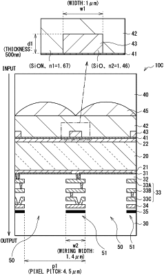
a drive substrate that includes a light-shielding region and a transmissive region;
a plurality of pixel electrodes that is transmissive and at a position corresponding to the transmissive region on the drive substrate;
a counter substrate opposite to the drive substrate with the plurality of pixel electrodes and the liquid crystal layer therebetween;
a first layer between the counter substrate and the liquid crystal layer, wherein the first layer includes a material having a first refractive index; and
a second layer in at least a portion of a region corresponding to the light-shielding region in the first layer, wherein
the second layer includes a material having a second refractive index lower than the first refractive index, and has a rectangular cross-sectional shape in a thickness direction, and
the second layer guides entering light to the plurality of pixel electrodes by a diffraction action.
|