| CPC G02F 1/133345 (2013.01) [G02F 1/133388 (2021.01); G02F 1/1334 (2013.01); G02F 1/1337 (2013.01); G02F 1/13394 (2013.01); G02F 1/134309 (2013.01); G02F 1/136286 (2013.01); G02F 2201/50 (2013.01)] | 7 Claims |
|
1. A display device comprising:
a display panel including
an array substrate,
a counter substrate, and
a liquid crystal layer between the array substrate and the counter substrate; and
a light source disposed along a side surface of the display panel,
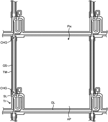
wherein the array substrate comprises, in a display region:
a plurality of signal lines arranged with spaces in a first direction;
a plurality of scanning lines arranged with spaces in a second direction;
a grid-shaped organic insulating layer that extends along the scanning lines and the signal lines on the array substrate and overlies the scanning lines and the signal lines;
a plurality of pixel electrodes provided in respective regions surrounded by the scanning lines and the signal lines; and
a first orientation film that covers the pixel electrodes,
wherein a portion of each of the pixel electrodes is disposed above and overlaps a slant surface of the organic insulating layer, and
wherein the counter substrate comprises:
a common electrode located in positions at least overlapping the respective pixel electrodes;
a protective film that has an insulating capability and a light transmitting capability and covers a side of the common electrode facing the array substrate at least in the display region; and
a second orientation film that covers the protective film.
|