| CPC G02B 6/4215 (2013.01) [G02B 5/201 (2013.01); G02B 6/4204 (2013.01); H01L 24/08 (2013.01); H01L 24/80 (2013.01); H01L 31/02327 (2013.01); H01L 31/105 (2013.01); H01L 2224/08145 (2013.01); H01L 2224/80895 (2013.01); H01L 2224/80896 (2013.01)] | 20 Claims |
|
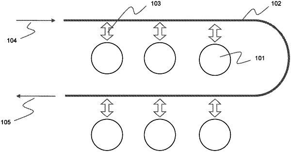
1. A semiconductor photodetector array sensor comprising:
a semiconductor photodetector array with a plurality of photodetector cells;
an optical waveguide structure with an optical waveguide, the optical waveguide being coupled to the semiconductor photodetector array electrically;
a light source coupled to the optical waveguide structure;
a photodetector sensor coupled to the optical waveguide structure;
a coupling structure at each of the plurality of photodetector cells, the coupling structure being configured to connect at least one of the plurality of photodetector cells and the optical waveguide structure to convert a photo event current at the at least one of the plurality of photodetector cells to an optical signal in the optical waveguide structure.
|