| CPC G02B 6/126 (2013.01) [G02F 1/035 (2013.01)] | 6 Claims |
|
1. An electronically controlled depolarizer based on a crossed-slit waveguide, the electronically controlled depolarizer comprising a horizontal-slit waveguide (1), a 45-degree polarization rotation waveguide (2), a crossed-slit waveguide (3) and a pair of modulation electrodes (4), wherein:
an output end of the horizontal-slit waveguide (1) is connected with an input end of the crossed-slit waveguide (3) through the 45-degree polarization rotation waveguide (2), the pair of modulation electrodes (4) are located at two sides of the 45-degree polarization rotation waveguide (2), respectively;
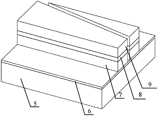
the horizontal-slit waveguide (1), the 45-degree polarization rotation waveguide (2) and the crossed-slit waveguide (3) are integrated on an upper surface of a basal layer which is formed by a silicon substrate (5) and a first silica buffer layer (6) along light transmission direction; the first silica buffer layer (6) is located on the silicon substrate (5); each of the horizontal-slit waveguide (1), the 45-degree polarization rotation waveguide (2) and the crossed-slit waveguide (3) comprises a first lithium niobate single crystal thin film layer (7), a second silica buffer layer (8) and a second lithium niobate single crystal thin film layer (9) from bottom to top in sequence;
each of the 45-degree polarization rotation waveguide (2) and the crossed-slit waveguide (3) has a vertical slit which penetrates through the first lithium niobate single crystal thin film layer (7), the second silica buffer layer (8) and the second lithium niobate single crystal thin film layer (9), and is filled with air; the vertical slit which is provided in the 45-degree polarization rotation waveguide (2) is formed by extending from a side edge of an input end of the 45-degree polarization rotation waveguide (2) to a middle portion of an output end thereof; the vertical slit which is provided in the crossed-slit waveguide (3) is formed by extending from a middle portion of an input end of the crossed-slit waveguide (3) to a middle portion of an output end thereof.
|