| CPC G02B 6/0076 (2013.01) [G02B 6/02395 (2013.01); G02B 6/02209 (2013.01)] | 20 Claims |
|
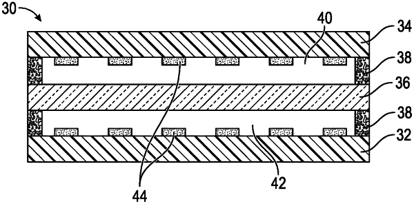
1. A stacked optical waveguide, comprising:
a glass substrate;
a plastic substrate having an optical structure, the plastic substrate secured to and spaced from the glass substrate;
another plastic substrate having another optical structure, the other plastic substrate secured to and spaced from the glass substrate such that the glass substrate is interposed between the plastic substrates;
an air gap disposed between the plastic substrate and the glass substrate; and
another air gap disposed between the other plastic substrate and the glass substrate, wherein the optical structures are encompassed by the respective air gap, and wherein the optical structures face the glass substrate.
|