| CPC G02B 27/0179 (2013.01) [G02B 5/32 (2013.01); G02B 6/4213 (2013.01); G02B 6/4215 (2013.01); G02B 27/0172 (2013.01); G02B 27/283 (2013.01); G03H 1/0248 (2013.01); G06F 3/013 (2013.01); G02B 2027/0138 (2013.01); G02B 2027/014 (2013.01); G02B 2027/0174 (2013.01); G02B 2027/0187 (2013.01)] | 16 Claims |
|
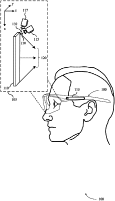
1. An electronic device comprising:
a light source configured to emit non-visible light;
a display configured to emit visible light;
a waveguide having first and second waveguide substrates, the first waveguide substrate having opposing first and second lateral surfaces, the second waveguide substrate having opposing third and fourth lateral surfaces parallel to the first and second lateral surfaces; and
an optical coupler disposed on the waveguide and comprising:
a grating medium disposed between the first and second waveguide substrates and contacting the second and third lateral surfaces,
a first volume holographic grating structure within the grating medium, the first volume holographic grating structure being configured to reflect the non-visible light about a reflective axis offset from a surface normal of the grating medium, and
a second volume holographic grating structure superimposed with the first volume holographic grating structure in the grating medium, the second volume holographic grating structure being configured to reflect the visible light about the reflective axis.
|