| CPC G01R 31/318533 (2013.01) [G01R 31/318536 (2013.01); G01R 31/318572 (2013.01); G01R 31/318597 (2013.01)] | 10 Claims |
|
6. A dual in-line memory module (DIMM) slot test method without series connection of test board through joint test action group (JTAG), comprising:
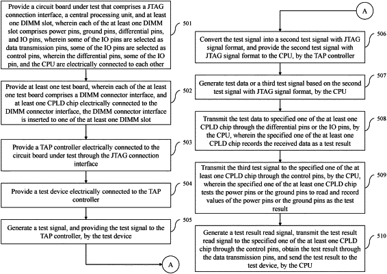
providing a circuit board under test that comprises a JTAG connection interface, a central processing unit, and at least one DIMM slot, wherein each of the at least one DIMM slot comprises power pins, ground pins, differential pins, and IO pins, wherein some of the IO pins are selected as data transmission pins, some of the IO pins are selected as control pins, wherein the differential pins, some of the IO pin, and the CPU are electrically connected to each other;
providing at least one test board, wherein each of the at least one test board comprises a DIMM connector interface, and at least one CPLD chip electrically connected to the DIMM connector interface, the DIMM connector interface is inserted to one of the at least one DIMM slot;
providing a TAP controller electrically connected to the circuit board under test through the JTAG connection interface;
providing a test device electrically connected to the TAP controller;
generating a test signal, and providing the test signal to the TAP controller, by the test device;
converting the test signal into a second test signal with JTAG signal format, and providing the second test signal with JTAG signal format to the CPU, by the TAP controller;
generating test data or a third test signal based on the second test signal with JTAG signal format, by the CPU;
transmitting the test data to specified one of the at least one CPLD chip through the differential pins or the IO pins, by the CPU, wherein the specified one of the at least one CPLD chip records the received data as a test result;
transmitting the third test signal to the specified one of the at least one CPLD chip through the control pins, by the CPU, wherein the specified one of the at least one CPLD chip tests the power pins or the ground pins to read and record values of the power pins or the ground pins as the test result; and
generating a test result read signal, transmitting the test result read signal to the specified one of the at least one CPLD chip through the control pins, obtaining the test result through the data transmission pins, and sending the test result to the test device, by the CPU.
|