| CPC G01R 31/2886 (2013.01) [H01L 24/08 (2013.01); H01L 25/0657 (2013.01); H01L 27/14634 (2013.01); H01L 27/14636 (2013.01); H01L 24/06 (2013.01); H01L 2224/06517 (2013.01); H01L 2224/08145 (2013.01); H01L 2225/06544 (2013.01)] | 11 Claims |
|
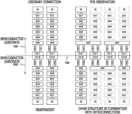
1. A semiconductor device, comprising:
a first semiconductor substrate;
a second semiconductor substrate;
a connection member that is electrically connected on joint surfaces of the first semiconductor substrate and the second semiconductor substrate to form at least one connection line that extends over the first semiconductor substrate and the second semiconductor substrate,
wherein the first semiconductor substrate and the second semiconductor substrate are bonded together on the joint surfaces;
a power supply terminal connected to one end of the at least one connection line; and
an observation terminal connected to another end of the at least one connection line.
|