| CPC G01N 21/9505 (2013.01) [G01N 21/9503 (2013.01); G01N 2201/061 (2013.01)] | 25 Claims |
|
1. A semiconductor edge and bevel inspection tool system of a wafer comprising:
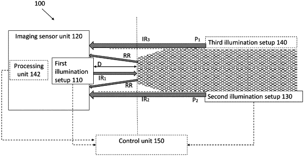
a first illumination setup being capable of facing a wafer edge and being configured and operable to generate a first illumination radiation along a first illumination axis and to direct at least a portion of the first illumination radiation towards an edge and bevel region of the wafer;
an imaging sensor unit defining a collection optical axis being configured and operable to collect light radiation and to generate sensing data thereof;
and a second illumination setup being configured to be capable of being placed facing said imaging sensor unit and being configured and operable to generate a second illumination radiation along a second illumination axis and to direct at least a portion of the second illumination radiation in a direction substantially parallel to the wafer plane toward said imaging sensor, wherein at least a portion of the second illumination radiation is configured for interacting with at least a portion of the edge and bevel region, wherein the first and the second illumination radiations have substantially opposite directions and wherein second illumination setup has different radiation parameters than the first illumination setup;
wherein said imaging sensor unit is configured and operable to collect a second illumination radiation directed towards said imaging sensor unit by said second illumination setup, as well as a reflected illumination radiation reflected from the edge and bevel region, wherein the reflected illumination radiation is created by the first illumination setup; such that the sensing data is indicative of a boundary between the wafer plane and that of the edge and bevel region.
|