| CPC G01N 21/9501 (2013.01) [G01B 11/0616 (2013.01); G01N 21/211 (2013.01)] | 20 Claims |
|
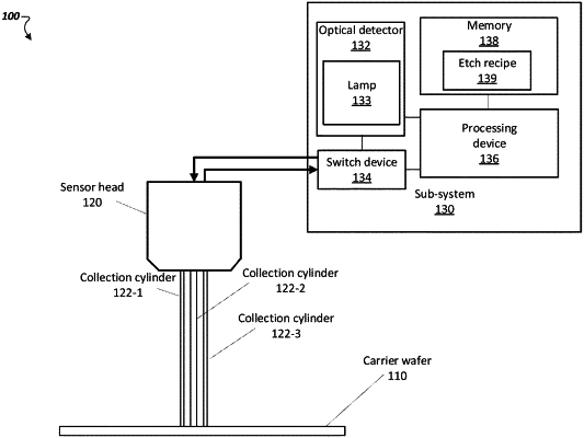
1. A system comprising:
a memory storing instructions to facilitate an etch recipe development process; and
at least one processing device operatively coupled to the memory, wherein the instructions, upon execution by the at least one processing device, cause the at least one processing device to facilitate the etch recipe development process by performing operations comprising:
obtaining, from an optical detector, first material thickness data for a first material and second material thickness data for a second material resulting from an iteration of an etch process using an etch recipe, wherein the first material is located at a first reflectometry measurement point and the second material is located at a second reflectometry measurement point different from the first reflectometry measurement point; and
determining one or more etch parameters based on at least the first material thickness data and the second material thickness data.
|