| CPC G01C 19/725 (2013.01) | 3 Claims |
|
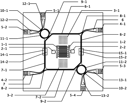
1. A chip-level resonant acousto-optic coupled solid state wave gyroscope, comprising a substrate and a gyroscope structure placed on the upper surface of the substrate,
the substrate includes, from top to bottom:
a lithium niobate crystal layer, a silicon dioxide crystal layer, a lithium niobate crystal layer; or
a lithium niobate crystal layer, a silicon dioxide crystal layer, a lithium niobate layer; or
a lithium niobate crystal layer, a silicon dioxide crystal layer, and a silicon crystal layer;
the gyroscope structure includes three parts: an acoustic sensitive module, an optical detection module and a phase modulation module,
the acoustic sensitive module is located in the middle of the gyroscope, and the acoustic sensitive module includes:
an interdigitated transducer composed of first interdigital fingers (1-1) and second interdigital fingers(1-2) formed by sputtering metal on surface of the uppermost thin film layer of the substrate; and
a first array of metallic pillars (3-1) and a second array of metallic pillars (3-2) for sensitive angular velocity formed by secondary sputtering metal on the surface of the uppermost thin film layer of the substrate, the first array of metallic pillars (3-1) consists of a plurality of metal columns, and the second array of metallic pillars (3-2) consists of a plurality of metal columns,
the optical detection module is located around the acoustic sensitive module, and the optical detection module includes:
a first input grating coupler (4-1) at a first light source input end and a second input grating coupler (4-2) at a second light source input end formed by etching on the surface of the uppermost thin film layer of the substrate;
a first output grating coupler (5-1), a second output grating coupler (5-2), a third output grating coupler (5-3) and a fourth output grating coupler (5-4) at a signal output end formed by etching on the surface of the uppermost thin film layer of the substrate;
a first input optical waveguide (6) at the first light source input end, a second input optical waveguide (7) at the second light source input end, respectively formed by etching on the surface of the uppermost thin film layer of the substrate;
a first optical waveguide (12-1), a second optical waveguide (12-2), a third optical waveguide (13-1) and a fourth optical waveguide (13-2) at the signal output end, respectively formed by etching on the surface of the uppermost thin film layer of the substrate; and
a first micro-ring resonant cavity (11-1) and a second micro-ring resonant cavity (11-2) formed by etching on the surface of the uppermost thin film layer of the substrate,
wherein, the first input optical waveguide (6) at the first light source input end is divided into a first optical waveguide branch (6-1) and a second optical waveguide branch (6-2) with the same structure by a fifth coupler (8-1);
the second input optical waveguide (7) at the second light source input end is divided into a third optical waveguide branch (7-1) and a fourth optical waveguide branch (7-2) with the same structure by a sixth coupler (8-2);
the first optical waveguide branches (6-1) and the third optical waveguide branch (7-1) are connected to each other via a first coupler (9-1) and the first micro-ring resonant cavity (11-1);
the second optical waveguide branches (6-2) and the fourth optical waveguide branch (7-2) are connected to each other via a second coupler (9-2) and the second micro-ring resonant cavity (11-2);
the phase modulation module includes two phase modulation modules respectively symmetrical with respect to the acoustic sensitive module, and placed on opposite sides of two optical waveguide branches in the optical detection module, the phase modulation module includes:
a first pair of phase modulation electrodes (14-1 and 14-2) on opposite sides of the third optical waveguide branch (7-1), formed by sputtering metal on the surface of the uppermost thin film layer of the substrate; and
a second pair of phase modulation electrodes (15-1 and 15-2) on opposite sides of the second optical waveguide branch (6-2), formed by sputtering metal on the surface of the uppermost thin film layer of the substrate.
|