| CPC C09K 11/621 (2013.01) [C08J 5/18 (2013.01); C09K 11/025 (2013.01); G02B 1/002 (2013.01); G02F 1/133603 (2013.01); G02F 1/133614 (2021.01); B82Y 20/00 (2013.01); B82Y 30/00 (2013.01); B82Y 40/00 (2013.01); C08J 2329/10 (2013.01); G02F 2202/36 (2013.01)] | 19 Claims |
|
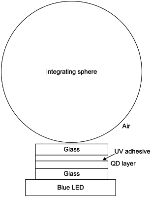
1. A method of preparing a film comprising Ag, In, Ga, and S (AIGS) nanostructures, comprising:
admixing at least one organic resin with AIGS nanostructures and at least one ligand to form an admixture;
preparing a first film comprising the admixture on a first barrier layer;
curing the film by UV irradiation and/or baking; and
encapsulating the first film between the first barrier layer and a second barrier layer;
wherein the encapsulated film exhibits a photon conversion efficiency (PCE) of greater than 32% at a peak emission wavelength of about 480-545 nm, when excited using a blue light source with a wavelength of about 450 nm;
wherein the nanostructures have an emission spectrum with a full width half maximum (FWHM) of less than 40 nm, and wherein the average diameter of the nanostructures is less than 10 nm by TEM.
|