| CPC B60R 11/04 (2013.01) [B60R 2011/0026 (2013.01)] | 29 Claims |
|
1. An imager assembly for a vehicular camera module, the imager assembly comprising:
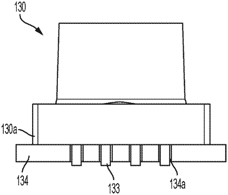
an imager circuit board;
wherein the imager circuit board has a first side and a second side opposite the first side, and wherein the second side is separated from the first side by a thickness dimension of the imager circuit board;
an imager disposed at the first side of the imager circuit board, the imager comprising a two dimensional imaging array of at least one million photosensor elements arranged in rows and columns;
a lens holder;
wherein the lens holder comprises a lens holding portion and an attaching portion;
wherein the lens holding portion of the lens holder accommodates a lens;
wherein the lens holder comprises a plurality of pins extending from the attaching portion and extending in a direction away from the lens holding portion of the lens holder;
wherein the lens holding portion extends from a first side of the attaching portion and the plurality of pins extend from a second side of the attaching portion that is opposite the first side;
wherein the attaching portion of the lens holder engages the first side of the imager circuit board to attach the lens holder to the imager circuit board;
wherein, with the attaching portion of the lens holder at the first side of the imager circuit board, individual pins of the plurality of pins are received at least partially through respective apertures of the imager circuit board;
wherein the apertures comprise a first set of apertures and a second set of apertures spaced apart along respective first and second side regions of the imager circuit board, and wherein the first side region is at an opposite side of the imager circuit board from the second side region, and wherein the pins comprise a first set of pins and a second set of pins, and wherein, with individual pins of the first set of pins received at least partially through respective apertures of the first set of apertures of the imager circuit board and individual pins of the second set of pins received at least partially through respective apertures of the second set of apertures of the imager circuit board, the first and second sets of pins are disposed at the imager circuit board along the opposite first and second side regions of the imager circuit board and spaced from opposite perimeter edges of the imager;
wherein the pins, as received at least partially through the respective apertures of the imager circuit board, locate the lens holder at the imager circuit board;
wherein, with the pins received at least partially through the apertures of the imager circuit board, the lens is aligned with the imager at the imager circuit board; and
wherein, with the pins received at least partially through the apertures of the imager circuit board, and with the lens aligned with the imager at the imager circuit board, the pins are fixedly attached at the imager circuit board.
|