| CPC H10K 71/00 (2023.02) [H10K 50/81 (2023.02); H10K 50/82 (2023.02); H10K 71/233 (2023.02)] | 7 Claims |

|
1. A display device comprising:
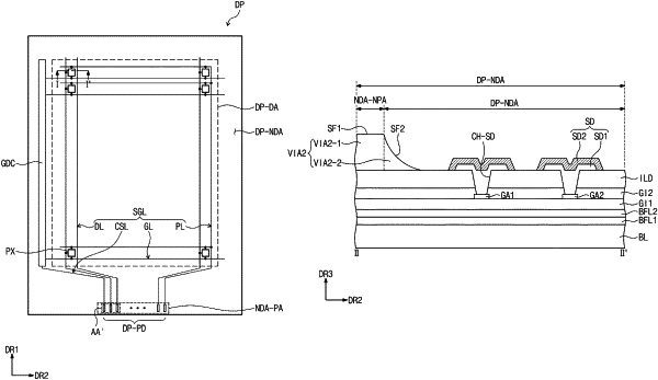
a display panel comprising:
a display area and a non-display area which is adjacent to the display area;
the non-display area including a pad area through which an electrical signal is provided to the display panel from outside thereof and a non-pad area which is between the display area and the pad area:
a base layer in each of the display area, the non-pad area and the pad area;
a first insulating layer on the base layer;
a pixel electrode in the display area, the pixel electrode facing the base layer with the first insulating layer therebetween;
a pad electrode in the pad area, the pad electrode facing the base layer with the first insulating layer therebetween;
a second insulating layer in the display area and facing the first insulating layer with the pixel electrode therebetween, the second insulating layer extending from the display area and into the non-display area to define:
a first portion corresponding to the non-pad area, and
a second portion extending from the first portion, toward the pad electrode and into the pad area, the second portion defining an upper surface which is furthest from the first insulating layer,
wherein the upper surface has a concave shape in cross-section; and
in the display area, a first electrode of a light emitting element, the first electrode facing the first insulating layer with the second insulating layer therebetween.
|