| CPC H10K 59/38 (2023.02) [H10K 50/856 (2023.02); H10K 50/858 (2023.02); H10K 50/87 (2023.02); H10K 59/12 (2023.02); H10K 71/00 (2023.02); H10K 2102/331 (2023.02)] | 13 Claims |
|
1. An electronic device, comprising
a first substrate,
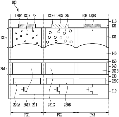
a plurality of light emitting elements each having a horizontal length and a vertical length which arc less than or equal to about 10 micrometers, each of the plurality of light emitting elements being disposed on the first substrate,
a quantum dot color filter layer disposed on the plurality of light emitting elements, the quantum dot color filter layer comprising:
a plurality of quantum dot color filters partitioned by a plurality of first partition walls so as to be overlapped with the plurality of light emitting elements, respectively; and
a first overcoat layer between the plurality of light emitting elements and the quantum dot color filter layer; and
a light guide layer between the plurality of light emitting elements and the first overcoat layer, and
the light guide layer comprises a plurality of second partition walls overlapped with the plurality of first partition walls.
|