| CPC H10K 59/351 (2023.02) [C07D 307/77 (2013.01); C09K 11/06 (2013.01); H10K 50/11 (2023.02); H10K 50/19 (2023.02); H10K 59/32 (2023.02); H10K 85/622 (2023.02); H10K 85/633 (2023.02); H10K 85/636 (2023.02); H10K 85/6574 (2023.02); C09K 2211/1007 (2013.01); C09K 2211/1011 (2013.01); C09K 2211/1014 (2013.01); C09K 2211/1088 (2013.01); H10K 50/131 (2023.02); H10K 59/40 (2023.02); H10K 85/626 (2023.02); H10K 2101/10 (2023.02); H10K 2101/27 (2023.02)] | 19 Claims |
|
1. A light-emitting device with a bottom emission structure, comprising:
a substrate;
a transistor comprising:
a first insulating layer over the substrate;
an oxide semiconductor layer over the first insulating layer;
a source electrode, a drain electrode, and a gate electrode over the oxide semiconductor layer; and
a second insulating layer over the oxide semiconductor layer, the source electrode, and the drain electrode;
an anode over the transistor;
a first light-emitting element configured to emit light through a first coloring layer so that blue light is extracted to an outside of the light-emitting device;
a second light-emitting element configured to emit light through a second coloring layer so that green light is extracted to the outside of the light-emitting device;
a third light-emitting element configured to emit light through a third coloring layer so that green light is extracted to the outside of the light-emitting device; and
a fourth light-emitting element,
wherein:
one of the source electrode and the drain electrode is electrically connected to the anode,
the anode is configured to function as a first electrode of one of the first to fourth light-emitting elements,
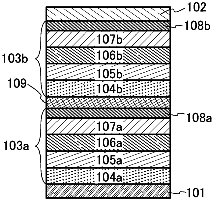
the first to fourth light-emitting elements comprise the same structure of a first EL layer and a second EL layer with a charge-generation layer therebetween,
the first EL layer includes a fluorescent substance configured to emit blue light, and
the second EL layer includes a phosphorescent substance configured to emit yellow light.
|