| CPC H10K 59/1315 (2023.02) [H10K 50/813 (2023.02); H10K 59/1213 (2023.02); H10K 59/1216 (2023.02); H10K 59/123 (2023.02); H10K 59/124 (2023.02); H10K 59/35 (2023.02); H01L 27/124 (2013.01); H01L 27/1248 (2013.01); H01L 27/1255 (2013.01)] | 10 Claims |

|
1. A display device, comprising:
a substrate;
a lower conductive pattern disposed on the substrate;
an active layer disposed on the substrate and including a plurality of active patterns including a semiconductor material;
a first conductive layer disposed on the active layer, the first conductive layer including a first gate electrode;
a second conductive layer disposed on the active layer, the second conductive layer including a first connecting electrode;
a third conductive layer disposed on the second conductive layer, the third conductive layer including a second connecting electrode;
a light-emitting layer disposed on the third conductive layer; and
a common electrode disposed on the light-emitting layer,
wherein
the first gate electrode overlaps the lower conductive pattern to form a first capacitor,
the common electrode is electrically connected to the second connecting electrode, and
the second connecting electrode is electrically connected to the first connecting electrode, and
the first connecting electrode, the second connecting electrode, and the common electrode transmit a first voltage, the display device further comprising
a first voltage line transmitting the first voltage,
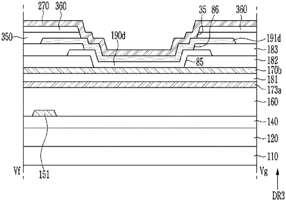
wherein a contact member, the second connecting electrode and the common electrode are sequentially stacked to extend across a contact hole on the first voltage line.
|