| CPC H10K 59/131 (2023.02) [G06F 3/0412 (2013.01); H01L 24/05 (2013.01); H10K 59/40 (2023.02); G06F 3/0443 (2019.05); G06F 3/0446 (2019.05); G06F 2203/04111 (2013.01); G06F 2203/04112 (2013.01); H01L 24/16 (2013.01); H01L 24/81 (2013.01); H01L 25/18 (2013.01); H01L 2224/05013 (2013.01); H01L 2224/05018 (2013.01); H01L 2224/0518 (2013.01); H01L 2224/05082 (2013.01); H01L 2224/05086 (2013.01); H01L 2224/05088 (2013.01); H01L 2224/05124 (2013.01); H01L 2224/05147 (2013.01); H01L 2224/05166 (2013.01); H01L 2224/05553 (2013.01); H01L 2224/05564 (2013.01); H01L 2224/05573 (2013.01); H01L 2224/05624 (2013.01); H01L 2224/05639 (2013.01); H01L 2224/05655 (2013.01); H01L 2224/05671 (2013.01); H01L 2224/05693 (2013.01); H01L 2224/16145 (2013.01); H01L 2224/16501 (2013.01); H01L 2224/81205 (2013.01); H01L 2224/81365 (2013.01); H01L 2924/01006 (2013.01)] | 27 Claims |
|
1. A display device comprising:
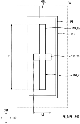
a substrate including an active area having a plurality of pixels and a non-active area disposed on a periphery of the active area and including a pad region;
a pad electrode disposed in the pad region and including a first pad electrode and a second pad electrode disposed on the first pad electrode; and
a first insulating pattern interposed between an upper surface of the first pad electrode and the second pad electrode,
wherein, when viewed in a plan view, an entirety of the first insulating pattern is positioned inside the first pad electrode, and a portion of the second pad electrode overlapping the first insulating pattern protrudes further from the substrate in a thickness direction than a portion of the second pad electrode not overlapping the first insulating pattern protrudes from the substrate in the thickness direction,
the second pad electrode directly contacts a portion of the upper surface of the first pad electrode that the first insulating pattern is not disposed on, and
when viewed in a plan view, an area of the second pad electrode is greater than an area of the first pad electrode.
|