| CPC H10K 59/131 (2023.02) [G09G 3/3233 (2013.01); H10K 59/124 (2023.02); G09G 2300/043 (2013.01); G09G 2300/0809 (2013.01); G09G 2300/0819 (2013.01); G09G 2300/0842 (2013.01); G09G 2300/0861 (2013.01); G09G 2310/0291 (2013.01)] | 14 Claims |
|
1. A display device, comprising:
a pixel area in which an image is displayed;
a peripheral area in which the image is not displayed,
wherein the pixel area and the peripheral area are separated from each other by a first curved line;
a substrate comprising a corner portion comprising a second curved line;
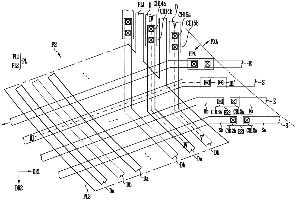
a plurality of pixels disposed in the pixel area on the substrate;
a plurality of data lines that supply data signals to the pixels;
a plurality of first power supply lines disposed in the pixel area; and
a second power supply line connected to the first power supply lines and disposed in the corner portion of the peripheral area,
wherein the plurality of data lines comprise first data lines and second data lines disposed in the corner portion,
wherein the first data lines comprise a first conductive layer, the second data lines comprise a second conductive layer different from the first conductive layer, the first power supply lines and the second power supply line comprise a third conductive layer different from the first and second conductive layers, and the first conductive layer is disposed between the second conductive layer and the third conductive layer in a cross-sectional view,
wherein, in the corner portion, the first data lines and the second data lines are alternately arranged with each other in the cross-sectional view such that the first data lines do not overlap the second data lines in the cross-sectional view,
wherein, in the corner portion, the first power supply lines are branched off from the second power supply line, the first power supply lines are disposed between the first data lines and the second data lines in a plan view,
wherein, in the corner portion, the second power supply line covers the first data lines and the second data lines, and
wherein the first curved line and the second power supply line have a same curvature.
|