| CPC H10K 59/122 (2023.02) [H10K 50/813 (2023.02); H10K 50/822 (2023.02); H10K 50/844 (2023.02); H10K 59/123 (2023.02); H10K 59/30 (2023.02); H10K 71/00 (2023.02); H10K 71/221 (2023.02); H10K 71/233 (2023.02)] | 8 Claims |
|
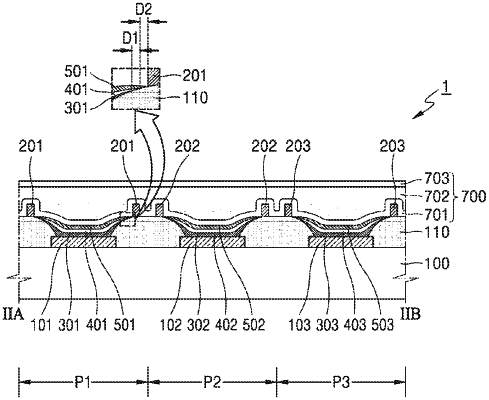
1. A method of manufacturing an organic light-emitting display apparatus, the method comprising:
forming, on a substrate, a pixel electrode and a pixel-defining film covering an edge of the pixel electrode;
forming, on the pixel-defining film, a bank protruding in a direction away from the substrate;
sequentially forming a liftoff layer and a photoresist on the pixel electrode, the pixel-defining film, and the bank;
forming an opening by patterning the liftoff layer and the photoresist, the opening exposing the pixel-defining film located on a top surface of the pixel electrode and within the bank;
sequentially depositing an intermediate layer comprising an emission layer, a counter electrode, and a passivation layer on the opening and the photoresist; and
removing a residue of the photoresist and the liftoff layer.
|