| CPC H10B 99/00 (2023.02) [G11C 11/405 (2013.01); G11C 16/0433 (2013.01); H01L 27/105 (2013.01); H01L 27/11803 (2013.01); H01L 27/124 (2013.01); H01L 27/1207 (2013.01); H01L 27/1225 (2013.01); H01L 27/1255 (2013.01); H01L 29/16 (2013.01); H01L 29/24 (2013.01); H01L 29/247 (2013.01); H01L 29/7869 (2013.01); H01L 29/78693 (2013.01); H01L 29/78696 (2013.01); H10B 41/20 (2023.02); H10B 41/70 (2023.02); H10B 69/00 (2023.02); G11C 2211/4016 (2013.01); H01L 21/8221 (2013.01); H01L 27/0688 (2013.01); H01L 29/7833 (2013.01); H10B 12/00 (2023.02)] | 15 Claims |
|
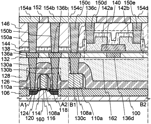
1. A semiconductor device comprising:
a first transistor; and
a second transistor,
wherein a channel formation region of the first transistor comprises silicon,
wherein a channel formation region of the second transistor comprises an oxide semiconductor,
wherein a first insulating layer is provided over the channel formation region of the first transistor,
wherein a first gate electrode of the first transistor is provided over the first insulating layer,
wherein the first gate electrode of the first transistor is electrically connected to one of a source and a drain of the second transistor via a first opening in a second insulating layer, a second opening in a third insulating layer, a third opening in a fourth insulating layer, a fourth opening in a fifth insulating layer, a fifth opening in the fifth insulating layer, and a sixth opening in the fourth insulating layer,
wherein the one of the source and the drain of the second transistor is in contact with a top surface of a layer which comprises the oxide semiconductor,
wherein a second gate electrode of the second transistor is provided below the channel formation region of the second transistor, and
wherein, in a cross-sectional view, the layer which comprises the oxide semiconductor extends beyond an end portion of the second gate electrode.
|