| CPC H10B 43/50 (2023.02) [H01L 23/562 (2013.01); H10B 41/27 (2023.02); H10B 41/50 (2023.02); H10B 43/27 (2023.02)] | 18 Claims |
|
1. A semiconductor memory device comprising:
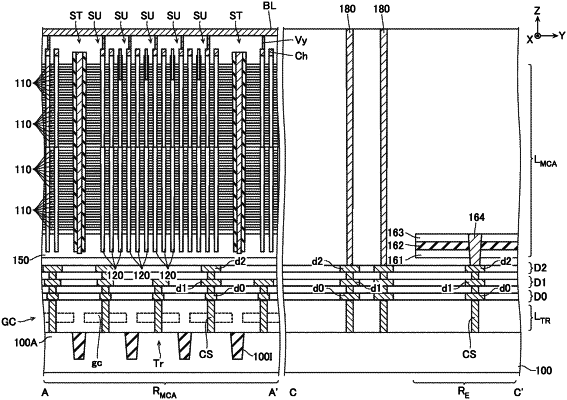
a semiconductor substrate, the semiconductor substrate comprising a first region including a plurality of memory cells, a second region provided between the first region and an edge of the semiconductor substrate, and a third region, the third region being provided between the first region and the second region;
a plurality of first conductive layers provided in the first region, the plurality of first conductive layers being aligned in a first direction intersecting a surface of the semiconductor substrate;
a first semiconductor layer provided in the first region, the first semiconductor layer extending in the first direction and facing the plurality of first conductive layers;
a second semiconductor layer provided in the first region, the second semiconductor layer being provided between the plurality of first conductive layers and the semiconductor substrate and being connected to the first semiconductor layer;
a third semiconductor layer and a fourth semiconductor layer provided in the second region, the third semiconductor layer and the fourth semiconductor layer being aligned in the first direction;
a second conductive layer provided in the second region, the second conductive layer being electrically connected to the third semiconductor layer, the fourth semiconductor layer, and the semiconductor substrate;
a fifth semiconductor layer provided in the third region, the fifth semiconductor layer extending in a second direction intersecting the first direction and comprising a portion formed continuously with the second semiconductor layer and a portion formed continuously with the third semiconductor layer; and
a sixth semiconductor layer provided in the third region, the sixth semiconductor layer extending in the second direction and comprising a portion formed continuously with the second semiconductor layer and a portion formed continuously with the fourth semiconductor layer,
the third region comprising a plurality of first portions and a plurality of second portions aligned alternately in the second direction,
in the plurality of first portions, the fifth semiconductor layer and the sixth semiconductor layer being separated in the first direction, and
in the plurality of second portions, the fifth semiconductor layer and the sixth semiconductor layer being electrically connected.
|