| CPC H10B 43/35 (2023.02) [H01L 21/0214 (2013.01); H01L 21/02164 (2013.01); H01L 21/0217 (2013.01); H01L 21/0223 (2013.01); H01L 21/02326 (2013.01); H01L 29/1037 (2013.01); H01L 29/40117 (2019.08); H01L 29/4234 (2013.01); H01L 29/511 (2013.01); H01L 29/518 (2013.01); H10B 43/10 (2023.02); H10B 43/27 (2023.02); H01L 21/02252 (2013.01); H01L 21/02255 (2013.01)] | 14 Claims |
|
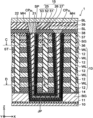
1. A semiconductor memory device comprising:
a substrate;
a stacked body including a plurality of electrode members and a plurality of insulating members, each of the electrode members and each of the insulating members being stacked alternately in a first direction above the substrate;
a memory hole that extends in the stacked body in the first direction;
a first insulating member that is disposed to extend in the memory hole in the first direction;
a semiconductor member that is disposed between the stacked body and the first insulating member to extend in the first direction;
a charge storage member that is disposed between the semiconductor member and one of the plurality of electrode members; and
a second insulating member that is disposed between the semiconductor member and the charge storage member, the second insulating member including nitride, wherein
the plurality of electrode members includes a first electrode member and a second electrode member, the first electrode member and the second electrode member being arranged in the first direction,
a diameter of the memory hole at a position of the second electrode member is larger than a diameter of the memory hole at a position of the first electrode member in a second direction orthogonal to the first direction,
a thickness of the charge storage member at the position of the second electrode member is greater than a thickness of the charge storage member at the position of the first electrode member in the second direction, and
a thickness of the second insulating member at the position of the first electrode member is greater than a thickness of the second insulating member at the position of the second electrode member in the second direction.
|