| CPC H10B 43/27 (2023.02) [G11C 5/025 (2013.01); G11C 16/0483 (2013.01); G11C 16/26 (2013.01); H01L 23/498 (2013.01); H01L 23/49827 (2013.01); H01L 23/49838 (2013.01); H10B 41/20 (2023.02); H10B 43/30 (2023.02); G11C 2213/71 (2013.01); H10B 43/20 (2023.02)] | 22 Claims |
|
1. A semiconductor memory device, comprising:
a semiconductor substrate extending in a first direction, a second direction, and a third direction, the first, second, and third directions crossing one another;
a circuitry formed on the semiconductor substrate;
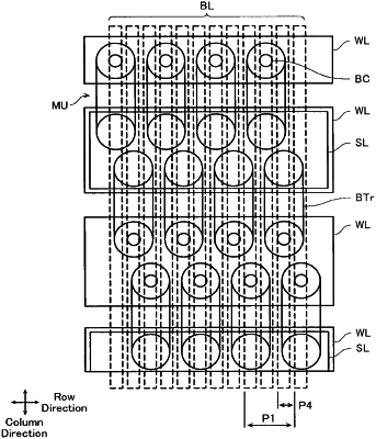
a source line formed above the semiconductor substrate in the third direction and extending in the first direction and the second direction;
a plurality of bit lines formed above the source line in the third direction, arranged in the second direction, and each extending in the first direction;
a memory cell array formed between the source line and the bit lines in the third direction;
a plurality of contacts connected between the bit lines and the memory cell array; and
a plurality of word lines formed between the source line and the bit lines, laminated in the third direction, and each extending in the first direction and the second direction,
wherein the memory cell array includes
a plurality of first memory pillars, each first memory pillar penetrating the word lines in the third directions to reach the source line, each first memory pillar having a first diameter, the first memory pillars being arranged in the second direction at first intervals,
a plurality of second memory pillars, each second memory pillar penetrating the word lines in the third directions to reach the source line, each second memory pillar having the first diameter, the second memory pillars being arranged in the second direction at the first intervals, each second memory pillar partially overlapping with adjacent two of the first memory pillars when viewed in the first direction, and
a plurality of third memory pillars, each third memory pillar penetrating the word lines in the third directions to reach the source line, each third memory pillar having the first diameter, the third memory pillars being arranged in the second direction at the first intervals, each third memory pillar overlapping with a corresponding one of the first memory pillars viewed in the first direction,
wherein the contacts include
a plurality of first contacts connected to ends of the first memory pillars, respectively, each first contact extending in the third direction, each first contact having a second diameter different from the first diameter,
a plurality of second contacts connected to ends of the second memory pillars, respectively, each second contact extending in the third direction, each second contact having the second diameter, and
a plurality of third contacts connected to ends of the third memory pillars, respectively, each third contact extending in the third direction, each third contact having the second diameter,
wherein the bit lines include
a plurality of first bit lines, each first bit line extending in the first direction, the first bit lines being arranged in the second direction, each first bit line being connected to a corresponding one of the first contacts and a corresponding one of the third contacts, and
a plurality of second bit lines, each second bit line extending in the first direction, the first bit lines being alternately arranged with the first bit lines in the second direction, each second bit line being connected to a corresponding one of the second contacts, and
wherein the circuitry includes
a first sense amplifier circuit connected to a part of the bit lines and overlapping with one part of the memory cell array when viewed in the third direction, and
a second sense amplifier circuit provided apart from the first sense amplifier circuit, connected to another part of the bit lines and overlapping with another part of the memory cell array when viewed in the third direction.
|