| CPC H10B 43/27 (2023.02) [H10B 41/10 (2023.02); H10B 41/27 (2023.02); H10B 43/10 (2023.02)] | 3 Claims |

|
1. A method for manufacturing a semiconductor storage device, the method comprising:
forming a predetermined film;
forming a plurality of holes penetrating the predetermined film;
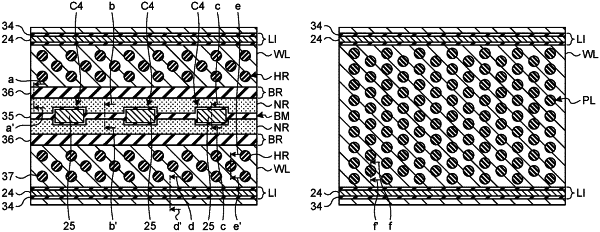
performing etching processing on the plurality of holes and a groove that couples the plurality of holes together with a width smaller than widths of the plurality of holes, to a predetermined depth of the predetermined film;
forming a sidewall layer on sidewalls of the plurality of holes and a sidewall of the groove to close the groove; and
further performing etching processing on the plurality of holes to penetrate the predetermined film, wherein
at a time of forming the predetermined film, forming the predetermined film as a first stacked body in which a plurality of first insulating layers and a plurality of second insulating layers are stacked alternately, and
at a time of forming the plurality of holes penetrating the predetermined film, forming a pair of first slits and a pair of second slits to penetrate the first stacked body, the pair of first slits having a longitudinal direction along a surface of each of layers of the first stacked body and having a width larger than a width of the groove, the pair of second slits having a longitudinal direction in a first direction and having a width larger than the width of the groove at positions on both sides of the pair of first slits separated from the pair of first slits.
|