| CPC H10B 43/27 (2023.02) [H01L 23/5226 (2013.01); H10B 41/10 (2023.02); H10B 41/27 (2023.02); H10B 43/10 (2023.02)] | 17 Claims |
|
1. A three-dimensional (3D) semiconductor memory device, comprising:
a semiconductor substrate;
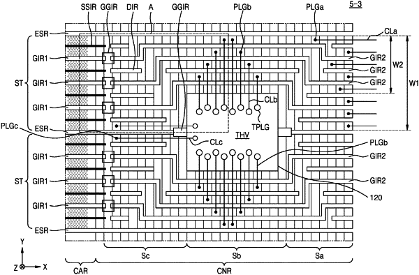
electrode structures, each of the electrode structures comprising a plurality of electrodes stacked on the semiconductor substrate, the electrode structures, as viewed in a plan view, extending in a first direction and being spaced apart from each other by electrode separation regions in a second direction perpendicular to the first direction, the first and second directions defining a plane that is parallel to an upper surface of the semiconductor substrate, wherein the plurality of electrodes in each of the electrode structures, as viewed in a cross-sectional view, are stacked on the semiconductor substrate in a third direction perpendicular to the first and second directions;
ground select gate electrodes comprising lowermost electrodes among the plurality of electrodes of the electrode structures; and
at least one ground select gate cutting region that overlaps at least a corresponding one of the electrode separation regions on a level of the ground select gate electrodes in the third direction, as viewed in a plan view, and electrically isolates the ground select gate electrodes from each other;
wherein the plurality of electrodes in each of at least a subset of the electrode structures are spaced apart from each other in the second direction by one or more gate isolation regions, the gate isolation regions comprising a first end portion on the level of the ground select gate electrodes;
wherein the gate isolation regions comprise a first isolation region comprising the first end portion and a second isolation region comprising a second end portion spaced apart from the first isolation region in the first direction, and
wherein the at least one ground select gate cutting region overlaps the first end portion of the first isolation region and the second end portion of the second isolation region in a third direction that is perpendicular to the first direction and the second direction.
|