US 11,917,820 B2
Vertical semiconductor device and fabrication method thereof
Eun-Ho Kim, Suwon (KR); Eun-Joo Jung, Icheon (KR); Jong-Hyun Yoo, Suwon (KR); Ki-Jun Yun, Yongin (KR); and Sung-Hoon Lee, Icheon (KR)
Assigned to SK hynix Inc., Icheon (KR)
Filed by SK hynix Inc., Icheon (KR)
Filed on Jul. 6, 2021, as Appl. No. 17/368,630.
Application 17/368,630 is a continuation of application No. 16/570,089, filed on Sep. 13, 2019, granted, now 11,088,160.
Claims priority of application No. 10-2019-0030113 (KR), filed on Mar. 15, 2019.
Prior Publication US 2021/0335800 A1, Oct. 28, 2021
Int. Cl. H10B 43/20 (2023.01); H10B 43/10 (2023.01); H10B 43/30 (2023.01); H10B 43/40 (2023.01)
CPC H10B 43/20 (2023.02) [H10B 43/10 (2023.02); H10B 43/30 (2023.02); H10B 43/40 (2023.02)] 11 Claims
OG exemplary drawing
 
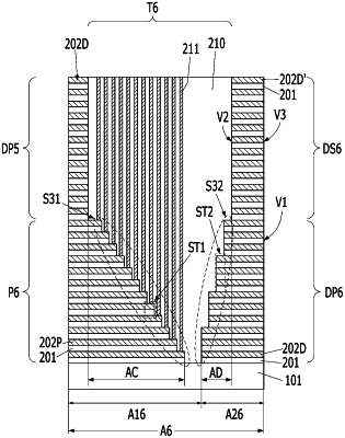
1. A vertical semiconductor device, comprising:
a substrate;
a gate pad stack and a dummy gate pad stack that are formed over the substrate and divided by an asymmetric stepped trench;
a first dummy stack formed over the gate pad stack; and
a second dummy stack formed over the dummy gate pad stack,
wherein the first dummy stack and the second dummy stack are divided by a vertical trench, and
wherein the first and second dummy stacks are electrically isolated structures.