| CPC H10B 41/27 (2023.02) [G11C 16/08 (2013.01); G11C 16/24 (2013.01); H01L 24/05 (2013.01); H01L 24/20 (2013.01); H01L 24/29 (2013.01); H01L 25/18 (2013.01); H01L 27/0296 (2013.01); H01L 29/0649 (2013.01); H01L 29/41741 (2013.01); H10B 41/10 (2023.02); H10B 41/35 (2023.02); H10B 41/41 (2023.02); H10B 43/10 (2023.02); H10B 43/27 (2023.02); H10B 43/35 (2023.02); H10B 43/40 (2023.02); H01L 2924/1431 (2013.01); H01L 2924/1438 (2013.01)] | 14 Claims |
|
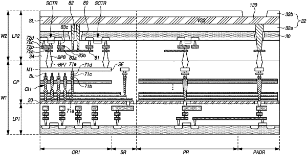
1. A memory device comprising:
a first wafer, and a second wafer stacked on and bonded to the first wafer,
wherein the first wafer comprises:
a cell structure including a memory cell array; and
a first logic structure disposed under the cell structure, and including a row control circuit,
wherein the second wafer comprises a second logic structure including a column control circuit,
wherein the memory cell array comprises a stack structure that is disposed on a source plate in a cell region and a slimming region, and bit lines disposed over the stack structure,
wherein the cell structure includes a source electrode that is coupled to the source plate through a contact structure passing through the stack structure, and
wherein the source electrode is disposed in the cell region of a wiring layer between the bit lines and the second wafer.
|