| CPC H10B 12/50 (2023.02) [G11C 11/4085 (2013.01); G11C 11/4097 (2013.01); H01L 23/5226 (2013.01); H10B 12/09 (2023.02); H10B 12/30 (2023.02); H10B 12/0335 (2023.02); H10B 12/482 (2023.02)] | 13 Claims |
|
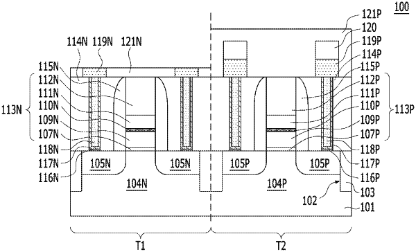
1. A semiconductor device, comprising:
a substrate including a memory cell region and a peripheral circuit region, the peripheral circuit region including a first peripheral circuit region including a first transistor and a second peripheral circuit region including a second transistor;
a storage node contact plug positioned in an upper portion of the substrate in the memory cell region;
a landing pad over the storage node contact plug;
a first metal wire coupled to the first transistor; and
a second metal wire coupled to the second transistor,
wherein a thickness of the landing pad and a thickness of the first metal wire are smaller than a thickness of the second metal wire, and
wherein a bottom portion of the landing pad, a bottom portion of the first metal wire, and a bottom portion of the second metal wire are positioned at the same level, and
an upper surface of the landing pad and an upper surface of the first metal wire are positioned at a lower level than an upper surface of the second metal wire.
|