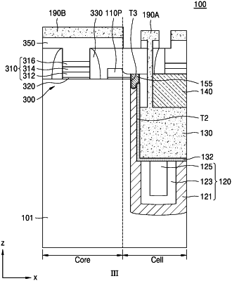
| CPC H10B 12/315 (2023.02) [H01L 23/5283 (2013.01); H10B 12/053 (2023.02); H10B 12/34 (2023.02); H10B 12/482 (2023.02); H10B 12/485 (2023.02); H10B 12/488 (2023.02)] | 20 Claims |

|
1. A manufacturing method of a semiconductor device, the method comprising:
defining an active region by forming a device isolation layer in a substrate by using a first mask;
forming a trench in the substrate crossing the active region and extending in a first direction, and by applying an insulating layer to form a first conductive layer filling a bottom portion of the trench, forming a buried word line;
forming a second mask filling a top portion of the trench on the word line;
by using the first mask and the second mask, recessing the device isolation layer such that side surfaces of a top portion of the active region are exposed;
forming a mask pattern exposing the first mask of a portion corresponding to the center of the active region, and by using the mask pattern, forming a contact hole by removing the exposed first mask and a top portion of the active region under the first mask;
forming a stop insulating layer and a gap fill insulating layer on an entire surface of the substrate, and by removing a portion of the gap fill insulating layer, forming a buffer insulating layer filling a space between two first masks adjacent to each other in the first direction;
forming a first contact by filling the contact hole with a second conductive layer; and
forming a bit line extending in a second direction perpendicular to the first direction on the word line, the bit line being connected to the first contact,
wherein the active region has a shape extending in an oblique direction with respect to the first direction, and
wherein the first contact is self-aligned to the active region by the first mask and the second mask that are arranged around the contact hole.
|