| CPC H10B 12/00 (2023.02) | 20 Claims |
|
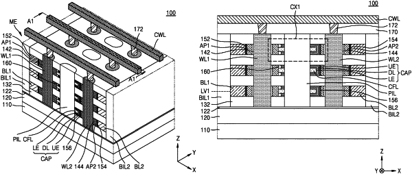
1. A semiconductor memory device comprising:
a first word line extending in a vertical direction over a substrate;
a second word line arranged over the substrate to be spaced apart from the first word line in a first horizontal direction, the second word line extending in the vertical direction;
a first semiconductor pattern having a ring-shaped horizontal cross-section that surrounds the first word line, the first semiconductor pattern constituting a portion of a first cell transistor;
a second semiconductor pattern having a ring-shaped horizontal cross-section that surrounds the second word line, the second semiconductor pattern constituting a portion of a second cell transistor;
a cell capacitor between the first semiconductor pattern and the second semiconductor pattern, the cell capacitor comprising a first electrode, a second electrode surrounding the first electrode, and a capacitor dielectric film between the first electrode and the second electrode;
a conductive filling layer contacting the first semiconductor pattern and the first electrode;
a capacitor contact layer contacting the second semiconductor pattern and the second electrode;
a first bit line arranged opposite the cell capacitor with respect to the first semiconductor pattern and extending in a second horizontal direction that is perpendicular to the first horizontal direction; and
a second bit line arranged opposite the cell capacitor with respect to the second semiconductor pattern and extending in the second horizontal direction.
|